Luxembourg
Layers to shuffle and recombine
FUTURE 3-5 explores layered semiconductor stacks as a flexible platform — materials and device fragments brought together in new combinations.
Public overview · concept
About
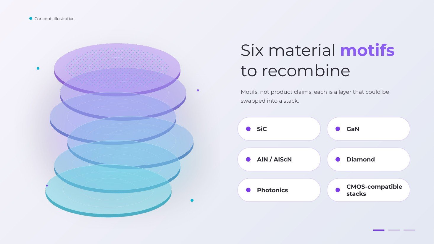
We work at the intersection of wide-bandgap materials and device design. The idea is simple: treat stacks as something you can recombine — opening room for new device architectures without locking into a single recipe.
- SiC
- GaN
- AlN / AlScN
- Diamond
- Photonics
- CMOS-compatible stacks
Stack recombination
Illustrative only: materials as layers that can be ordered, swapped and combined — the working metaphor for how FUTURE 3-5 thinks about device platforms.
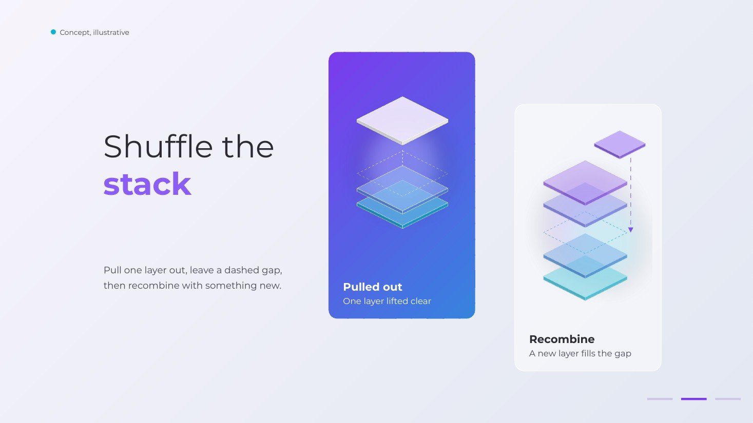
Public concept graphics from the FUTURE 3-5 deck — not process data or device specifications.
FAB35
A mini R&D fab in Luxembourg
FAB35 is our planned mini R&D facility. The name nods lightly to fab numbering and to a 2035 technology horizon — a place to build, test and iterate stacks at research scale.
- 1 Build Grow and assemble layered stacks at research scale
- 2 Test Characterise materials and device fragments
- 3 Iterate Recombine recipes toward CMOS-compatible windows
Contact
For general enquiries about FUTURE 3-5 and FAB35, use the contact details we share when we reach out, or ask via your usual channel with the team.
A public email address will be added once the domain mailbox is live.